

MCM packaged GPU begins to enter the era of Three Kingdoms
Source: UST WIRELESS Release time:10/06/2022
In recent years, GPU has become more and more important in the industry. Whether it is in high-performance computing or in the consumer level field, its stickiness to users is becoming stronger and stronger. NVIDIA’s popularity is due to its core GPU technology and products. In this case, the traditional giant Intel can’t sit still. Originally, it only produced integrated GPU graphics cards in the consumer level market. Changes in market demand have led Intel to set up an independent GPU R & D team, More and more resources have been invested to cope with the competition between NVIDIA and AMD, especially in the field of high-performance computing.
In the field of high-performance applications, the demand for controllable power consumption and cost of GPU is becoming higher and higher, which puts forward higher requirements for related technologies, including chip design methods, EDA tools, process technology, and packaging technology. In order to achieve an effective balance between high performance, power consumption, and cost, none of these technical links is indispensable. With the gradual "failure" of Moore’s law, the importance of advanced packaging technology is becoming more and more prominent, Intel, AMD and NVIDIA all see the importance of this link and continue to strengthen research and development. Especially recently, these three companies have disclosed important information on MCM (multi chip module) at the same time.
MCM into GPU
MCM is born to solve the problems of low integration and imperfect functions of a single chip. It uses SMD technology to form a variety of electronic module systems on a high-density multi-layer interconnection substrate with multiple die with high integration, high performance and high reliability to form a multi chip module. MCM has the following characteristics: the packaging delay time is reduced, and it is easy to realize high-speed module; Reduce the package size and weight of the whole machine / module; The system reliability is greatly improved.
In the past, MCM was mainly used for CPU and storage devices, especially in the CPU field. For example, IBM’s power4 dual core processors in the early days, namely MCM formed by four dual core power4 and additional L3 cache, Intel’s Pentium D (R & D Code: Presler), Xeon, AMD’s Zen 2 architecture ryzen (core code: Matisse), epyc processors, etc., are typical representatives of MCM applications.
In recent years, led by AMD, MCM Packaging Technology began to move towards GPU. The main reason for this is that the traditional graphics card is a PCB card with multiple GPUs, which requires a crossfire or SLI bridge to connect two independent graphics cards. Traditional SLI and crossfire ™ require PCIe bus to exchange data, texture, synchronization, etc. Due to the synchronization of rendering time between GPUs, in many cases, the traditional dual GPU graphics card, that is, two chips on a single PCB are interconnected by it, and each chip has its own VRAM. SLI or crossfire ™ consumes a lot of energy, and cooling is also a challenge, which has troubled engineers for a long time.
MCM GPU is a separate package, and its on-board bridge replaces the traditional crossfire or SLI bridge between two independent graphics cards.
In the field of high-performance computing applications, this MCM GPU has obvious advantages. It is also worth spending more time and energy on solving the software problems in packaging and interconnection to cope with the higher complexity of MCM design. At present, MCM GPU is mainly used in data center and cloud computing applications. With the continuous maturity of technology and the improvement of PC application performance, its application in the field of consumer electronics will also appear.
The big three
Amd was the first to introduce MCM Packaging Technology into GPU. In 2020, the company separated the GPU architecture of game cards and professional cards. The architecture of game cards is rDNA, while the architecture of professional cards is called cDNA. The first product is the insict mi100 series. In 2021, AMD’s Q2 financial report confirmed that cDNA 2 GPU had been shipped to customers. Its GPU core code was Aldebaran, which became AMD’s first product packaged with MCM and was prepared for the data center. On the PC side, after the introduction of the next generation rDNA 3 architecture in 2022, consumer radeon GPUs based on MCM will also appear.
Manufacturing a multi-chip computing GPU is similar to manufacturing a multi-core MCM CPU, such as a ryzen 5000 or threadripper processor. First, getting chips closer together can improve computing efficiency. AMD’s infinity architecture ensures high-performance interconnection, which is expected to make the efficiency of two chips close to that of one. Secondly, it is easier to batch produce multiple small chips using advanced technology than large chips, because small chips usually have fewer defects, so the output is better than that of large chips.
At the 2021 earnings conference call a few days ago, amd confirmed that there will be several important product releases this year, including the GPU based on rDNA 3 architecture, that is, the radeon RX 7000. At present, the latest graphics cards in this series will have three GPUs, namely Navi 31, Navi 32 and Navi 33. Among them, Navi 31 and Navi 32 will be packaged in MCM. Previously, it was rumored that the infinity cache of Navi 31 and Navi 32 will adopt the design of 3D stack and will be added to the MCD chip separately. Similar to the principle of 3D v-cache on Zen 3 architecture, the performance will be greatly improved.
Since the Navi 31 and Navi 32 adopt MCM Packaging, AMD will use two different processes. The GPU will use TSMC’s 5nm process, and the cache i/o chip will use TSMC’s 6nm process.
NVIDIA is also following up on MCM Packaging GPU.
In 2017, NVIDIA demonstrated the design scheme constructed by four small chips, which not only improved the performance, but also helped to improve the output (the yield of smaller chips would increase), but also allowed more computing resources to be gathered together. This multi chip design also helps to improve power supply efficiency and has better heat dissipation effect.
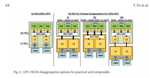
Recently, NVIDIA researchers published a technical article outlining the company’s exploration of MCM. NVIDIA’s current approach to MCM Packaging GPU is called "composable on package GPU" (Copa). The team described the advantages of Copa GPU, especially its ability to adapt to various types of deep learning workloads.
Because the traditional converged GPU solution is rapidly becoming less practical, researchers came up with the concept of copa-gpu. The converged GPU solution relies on the architecture composed of traditional chips, supplemented by the combination of high bandwidth memory (HBM), tensor core / matrix core, ray tracing (RT) and other special hardware.
Such hardware may be appropriate for some tasks, but inefficient in other situations. Unlike the current monolithic GPU design that combines all specific execution components and caches into one package, the copa-gpu architecture has the ability to mix / match multiple hardware blocks. In this way, it can better adapt to the dynamic workload and deep learning (DL) environment that high-performance computing can only present today.
This consolidation is more adaptable to multiple types of workloads, resulting in a higher level of GPU reuse. More importantly, for data scientists, this makes them more capable of using existing resources to break through potential boundaries.
For the data center and consumer market, NVIDIA will launch GPUs based on hopper architecture and ADA Lovelace architecture respectively. It is reported that the company will only use MCM technology on hopper architecture GPU. ADA Lovelace architecture GPU will still retain the traditional packaging design and will not introduce MCM multi chip packaging to consumer GPU like amd Navi 31 based on rDNA 3 architecture.
Recently, it was reported that the number of transistors of GH100 based on hopper architecture will reach 140billion, which is almost 2.5 times that of ga100 based on ampere architecture (54.2 billion) or AMD insight mi200 series based on cDNA 2 Architecture (58billion). It is said that the chip size of GH100 is close to 900mm ², 1000mm higher than the previous rumors ² Smaller than ga100 (862mm ²) And insict mi200 series (about 790mm ²) Larger. It is said that the GH100 is equipped with 288 SM, which can provide three times the performance of the A100 computing card.
It is reported that, as NVIDIA’s first GPU based on MCM technology, hopper architecture products will adopt TSMC 5nm process, support hbm2e and other connection features, and are expected to appear in mid-2022. The competitors will be Intel’s Xe HP architecture GPU and AMD’s cDNA 2 architecture products.
However, the above statement has not been officially confirmed. NVIDIA will hold the GTC 2022 Conference on March 21 this year. At that time, the hopper architecture and the corresponding acceleration card scheme may be announced.
As a latecomer to the independent GPU, Intel has also made frequent moves recently.
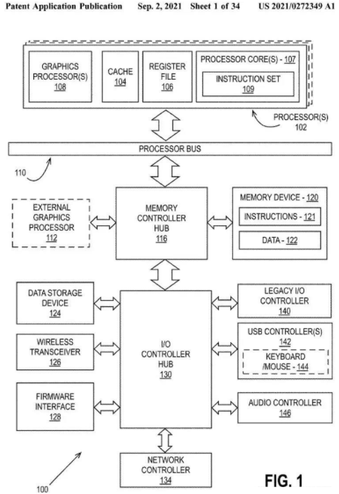
Recently, Intel announced a new patent that describes how multiple computing modules work together to perform image rendering, representing that Intel GPU will adopt MCM Packaging Technology to significantly improve operation efficiency.
Intel’s CPUs for the data center and the supercomputer Ponte Vecchio have used multi chip design and MCM Packaging Technology. In the new patent, Intel proposes a GPU image rendering solution, which integrates multiple chips into the same unit, solves problems such as manufacturing and power consumption, and optimizes scalability and connectivity.
At present, this kind of image rendering problem will be solved by algorithms such as alternate frame rendering (AFR) or scissor frame rendering (SFR). However, Intel is a chessboard format rendering integrated with the operation module and has distributed operation, which makes the multi chip design GPU more efficient. Although Intel did not describe the details of the architecture, it is expected that it is only a matter of time before Intel arc brand graphics cards are equipped with MCM Packaging Technology GPU.
epilogue
In terms of GPU R & D, Intel, AMD and NVIDIA are becoming more and more "synchronized". Especially in terms of process technology and packaging technology, the manufacturing process relies on TSMC, and packaging values MCM. AMD, which was originally the leading company in these two aspects, has less and less advantages. Especially in terms of MCM, NVIDIA and Intel have developed rapidly, not only in the field of high-performance computing, but also in the consumer market. Although amd first applied MCM technology to PCs, However, NVIDIA and Intel are also speeding up their progress, and it is believed that corresponding solutions will be launched soon.
MCM packaged GPU began to enter the era of Three Kingdoms.
Information about
- E-mailemily@ustwireless.com
- Phone00852-38449311
- Addressnew ship to/ship to address: UNIT NO.532B 5/F STAR HOUSE, NO.3 SALISBURY ROAD, TSIM SHA TSUI, KL, HongKong