

TSMC confirms that 2nm turns to nano chips, and CFET is promising in the future
Source: UST WIRELESS Release time:21/01/2021
According to foreign media eetimes, TSMC shared its process roadmap with a few media earlier. According to them, TSMC will launch the 2nm process using nano chip transistors in 2025. Looking forward to the future, the OEM is evaluating CFET and other process technologies to regard them as the "successor" of nano chips.
According to Kevin Zhang, vice president of TSMC business development, CFET is an option and is still in the R & D stage, so he can not provide any timetable.
TSMC’s technology roadmap shows that the new materials they are studying include tungsten disulfide. Kevin Zhang pointed out that this material provides better conductivity and more energy-saving calculation. He also added that what TSMC is still evaluating is carbon nanotubes, a material that can move electrons more effectively.
Kevin Zhang also pointed out that 3 nm will be a long node. There will be a lot of demand on this node. Customers who have higher requirements for computing energy efficiency can take the lead in turning to 2nm.
"3 nm and 2 nm will overlap [and] coexist for quite a long time," Kevin Zhang said.
Transistor selection after 3nm
Recently, several wafer factories announced that their mass production technology of 3nm or 2nm logic chips will shift from the mainstream FinFET process to nanosheet transistor architecture. In this paper, IMEC will review the early development of nano chip transistors and look forward to its new generation architecture, including forksheet and complementary field effect transistor (CFET).
The chip industry has never been eager to adopt a new transistor architecture for mass production, because it will bring complex new situations and investment costs. But recently, the public statements of companies such as Samsung, Intel, TSMC and IBM have shown that we are facing a key turning point in process technology.
From 2022 or 2023, these large semiconductor manufacturers will gradually shift from the fin field effect transistor (FinFET) process that has been used for a long time, and introduce the transistor architecture in the form of nanosheets into the production planning of 3-nanometer or 2-nanometer logic chips.
This article will explain the main factors driving this historic turn. It will also introduce different generations of nano chip architectures, including nano chip, forksheet and complementary field effect transistor (CFET). At the same time, it will evaluate the individual competitive advantages of these architectures in the CMOS miniaturization process, and discuss the key process steps.
Considerations for transferring from FinFET to nano chip manufacturing process
In order to further miniaturize CMOS logic elements, the semiconductor industry has invested a lot of effort to continuously reduce the size of logic standard cells. It is a practice to reduce the height of the standard unit. This value is defined as the product of the number of wires (or tracks) per standard cell and the metal layer spacing.
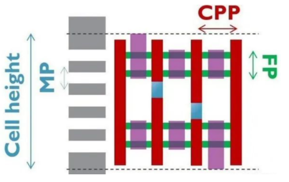
Figure 1: schematic diagram of logical standard cell layout: Contact poly pitch (CPP), fin pitch (FP), metal pitch (MP), and standard cell height.
By reducing the number of tracks, the height of the standard unit can be shortened. In terms of FinFET architecture, the new generation design is to achieve miniaturization by reducing the number of fins, from three fins to two fins, forming 7.5-rail and 6-rail standard units respectively. Taking the 6-rail design as an example, it means that each standard unit height can accommodate 6 metal conductors. However, if the number of fins is reduced while maintaining the same size, the driving current will be reduced and the variability will be increased. Therefore, in order to compensate for these performance losses, the configuration of the fins will be lengthened, and finally the design of single fin 5-rail can be realized.
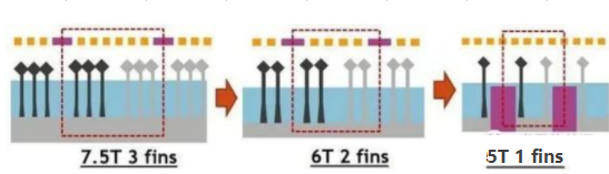
Figure 2: in order to further miniaturize the standard unit, the FinFET architecture must reduce the number of fins. The fin configuration of the new generation design will be longer, thinner and tighter, the driving current will be reduced, and the variability will also be increased.
However, it is very difficult to further improve the driving current of the single fin 5-rail FinFET element. At this time, it is the turn of the nano chip architecture. A wider effective channel width can be formed by vertically stacking the conductive channels of nanosheets with multiple single fin standard units. In this way, nanosheets can provide higher driving current than fins at the same size, which is the key advantage of continuously miniaturizing CMOS devices.
In addition, the nano chip architecture also provides flexibility to adjust the channel width, making the design more free. In other words, designers can choose not to increase the driving current, but to further reduce the component size and capacitance: using a narrow channel design can usually reduce the parasitic capacitance between layers.
Another notable feature of nanosheets over FinFET is the use of gate all around (GAA) structure. In this structure, the conductive channel is completely surrounded by a high dielectric coefficient material or a metal gate. Therefore, the gate can still show better channel control ability when the channel is shortened.
Key process modules
Just like the transition period from planar MOSFET to FinFET in the past, the current transition from FinFET to nano chip structure also faces new process integration challenges. Fortunately, nanosheets can be regarded as the natural evolution of FinFET, so many modules for optimizing and developing FinFET process can be used in the nanosheet process. This also makes it easier for the industry to accept the new architecture. Nevertheless, IMEC pointed out that there are still four key differences between FinFET and nano chip manufacturing processes, requiring special research and development of innovative technologies.
Firstly, in order to construct the contour of the channel, the nano sheet structure will use silicon (SI) and silicon germanium (SiGe) for multi-layer epitaxial growth. Due to the use of different growth materials, there is also a corresponding gap mismatch problem, which makes the traditional CMOS process no longer applicable. In the stack with multi-layer architecture, SiGe is a sacrificial layer, which will be removed in the step of removing the replacement metal gate (RMG) and releasing the channel. Then, the whole stack will be graphically made into fins with high aspect ratio. Therefore, how to ensure the configuration of nano sheets is a challenge.
IMEC put forward a set of key optimization schemes at the 2017 international electronic components Conference (IEDM). A low heat budget shallow trench isolation process was used to introduce a liner. As a result, oxidation induced fin deformation could be effectively suppressed. This also strengthens the shape control of the nanosheets, thereby improving the performance of the components, including DC and AC efficiency. The former refers to increasing the driving current, while the latter refers to accelerating the switching speed at the same power. The first application case of the new nano chip manufacturing process is the ring oscillator circuit, whose AC efficiency is successfully upgraded by shorter gate delay.
The second difference between Nano chip structure and FinFET is that a lining layer needs to be introduced, that is, a dielectric layer is added to isolate the gate and the source / sink, so as to reduce the capacitance. In this process step, the outside of the SiGe layer will form a depression after transverse etching, and then these small holes will be filled with dielectric material. The integrated lining is the most complicated step in the nano chip manufacturing process. It has strict requirements on the etching technology and requires high selection ratio and accurate lateral control. This challenge has attracted the attention of research teams everywhere, including IMEC.
The third difference is that the nano sheet manufacturing process includes the step of releasing channels, after which the nano sheets will be separated from each other. The method is to remove the silicon germanium layer by etching. In the process, a high degree of selectivity is required to keep a small amount of germanium between the nanosheets and reduce the surface roughness of the silicon material. In addition, in order to avoid the adhesion of these miniaturized nanosheets, the static friction must be controlled. IMEC has carried out basic research on different etching methods, including dry and wet processes. At present, the results can greatly help to solve the above problems.
The last point is the integration of alternative metal gates, including the deposition of metal in the gap around and between the nanosheets and the patterning. IMEC pointed out in 2018 that in order to shorten the vertical spacing between nanosheets, it is very important to import metal materials with work function modulation range. The IMEC team also showed relevant achievements, shortening the vertical spacing of nano chips from 13nm to 7Nm. As a result, the AC efficiency was improved by 10%. It can be seen that the miniaturization is important to replace the metal gate.
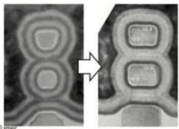
Figure 3: optimization for the surrounding gate nanosheets of the vertical stack: (left) material row control, (right) vertical gap reduction.
Fork piece on stage
The fastest and most effective way to improve the DC efficiency of nanosheets is to increase the effective width of channels. However, it is not easy to achieve this under the general nano chip architecture. The main problem is that a wide range of gap must be reserved between n-type and p-type MOSFETs. Therefore, when the height of the standard cell is reduced, it will be more and more difficult to accommodate a wider effective channel, and the N-P gap will become smaller when the metal is patterned.
The fork type plate can solve the problem of N-P gap. This architecture was proposed by IMEC, and its first appearance was the SRAM miniaturization research published at the 2017 international electronic components Conference (IEDM), and it was used as the miniaturization solution of the logical standard unit in the research published at the 2019 conference. The fork chip process has achieved the goal of shortening the N-P gap. Before the gate is patterned, a layer of dielectric wall is introduced between the n-type and p-type components, and the patterned hard mask can be carried out on the dielectric wall. In contrast, the nano chip process places it at the bottom of the gate channel.
The introduction of the dielectric wall can greatly reduce the distance between n-type and p-type components, increase the effective width of the channel, and improve the driving current, that is, the DC efficiency. In addition, n-p spacing miniaturization can not only maximize the effective width of the channel, but also choose to reduce the number of tracks of the standard unit from 5 to 4. This requires the development of innovative technologies for the rear and middle processes, and the use of new miniature accelerators, such as the buried power rail and the self-aligned gate contact.
According to the simulation results, the AC efficiency of the fork sheet may be better than that of the nano sheet, increasing by 10%. In this regard, the IMEC team also explained that since the overlapping area between the gate and the drain is reduced, the miller capacitance or parasitic capacitance will also be reduced, thereby improving the switching speed of the components, which may also help to manufacture more energy-efficient components.
From the point of view of the process, the fork shaped chip is an advanced and improved version derived from the nano chip. The main differences include the introduction of the dielectric wall, the improvement of the epitaxial growth of the inner liner and the source / sink, and the further miniaturization to replace the metal gate. At the 2021 international VLSI symposium, IMEC demonstrated for the first time the field effect components integrated in the 300mm nano chip process, and disclosed their electrical data. Among them, the element has successfully integrated the metal gate of double work function within the N-P spacing of only 17nm, showing the greatest advantage of adopting the fork chip architecture.
However, the fork chip architecture also has electrostatic problems. The most concerned feature of the nano chip is its four-sided gate structure, which can greatly improve the static control ability of the channel. However, the fork chip seems to have stepped back and changed to a three-sided gate structure. Nevertheless, IMEC integrated the nano chip and the fork chip on the same wafer in the above experiments. It was found that the fork chip showed a short channel control capability comparable to the nano chip when the gate length was 20nm (SS sat = 66-68mv).
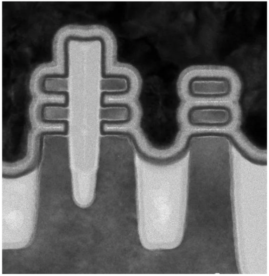
Figure 4: transmission electron microscope (TEM) images of nanosheets and forks integrated into the same wafer. Among them, the N-P spacing of the fork is only 17nm, and the metal gate with double work function is successfully integrated.
Long distance runner of nano chip series: CFET architecture
To maximize the effective channel width, complementary field effect transistor (CFET) is a feasible architecture to stack n-type and p-type components vertically. In other words, the N-P spacing changes to the vertical direction, so it is not necessary to consider the height limit of the standard unit. The new space released after the vertical stack of components can not only further extend the channel width, but also be used to reduce the number of tracks to less than 4.
The simulation results show that the CFET architecture can help the future logic elements or SRAM continue to miniaturize. The channel configuration can be n-type or p-type fins, or n-type or p-type nanosheets. Finally, CFET architecture will be the most perfect architecture in the nano chip series and become the best choice for CMOS devices.
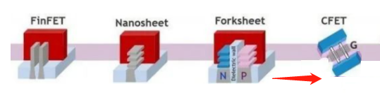
Figure 5: evolution process of CMOS component architecture, which is followed by FinFET, nano chip, fork chip and CFET.
Because the CFET architecture must stack NMOS and PMOS vertically, the process will be more complex. There are two vertical integration schemes, namely, monolithic and sequential, which have their own advantages and disadvantages. In this regard, IMEC has developed relevant process modules and integration schemes, quantified the performance of these processes in terms of power consumption, performance and size, and evaluated their technical difficulties.
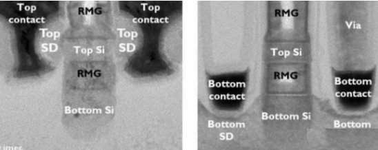
Figure 6: transmission electron microscope (TEM) image of CFET element with monolithic process: (left) element top (right) element bottom.
Monolithic CFET: low cost, but complex vertical integration process
The first step in manufacturing monolithic CFET is the epitaxial growth of the bottom channel, the deposition of the middle sacrificial layer, and finally the growth of the top channel. If nano chip architecture is to be adopted, silicon fins or multi-layer stacks of silicon or silicon germanium can be used for the manufacture of channels from bottom to top.
No matter which configuration is selected above, components will form an ultra-high aspect ratio architecture after vertical stacking. Therefore, in the subsequent graphical multi-channel steps, including fins, gates, lining and source / sink contacts, will face a severe test. For example, the steps of integrating and replacing metal gates are particularly complicated, because n-type and p-type components require metal materials with different work functions.
At the 2020 international VLSI symposium, IMEC demonstrated for the first time the integrated components with monolithic CFET architecture by using optimized process modules.
Sequential CFET: channel can mix materials, but wafer transfer is difficult
The sequential CFET process consists of several modules. First, the components will be manufactured from the bottom up to the contact, then the dielectric to dielectric wafer bonding technology will be used to cover a layer of non graphical semiconductor layer, and finally the top components will be integrated and the upper and lower gates will be connected. The whole process is based on the middle and rear sections
According to Kevin Zhang, vice president of TSMC business development, CFET is an option and is still in the R & D stage, so he can not provide any timetable.
TSMC’s technology roadmap shows that the new materials they are studying include tungsten disulfide. Kevin Zhang pointed out that this material provides better conductivity and more energy-saving calculation. He also added that what TSMC is still evaluating is carbon nanotubes, a material that can move electrons more effectively.
Kevin Zhang also pointed out that 3 nm will be a long node. There will be a lot of demand on this node. Customers who have higher requirements for computing energy efficiency can take the lead in turning to 2nm.
"3 nm and 2 nm will overlap [and] coexist for quite a long time," Kevin Zhang said.
Transistor selection after 3nm
Recently, several wafer factories announced that their mass production technology of 3nm or 2nm logic chips will shift from the mainstream FinFET process to nanosheet transistor architecture. In this paper, IMEC will review the early development of nano chip transistors and look forward to its new generation architecture, including forksheet and complementary field effect transistor (CFET).
The chip industry has never been eager to adopt a new transistor architecture for mass production, because it will bring complex new situations and investment costs. But recently, the public statements of companies such as Samsung, Intel, TSMC and IBM have shown that we are facing a key turning point in process technology.
From 2022 or 2023, these large semiconductor manufacturers will gradually shift from the fin field effect transistor (FinFET) process that has been used for a long time, and introduce the transistor architecture in the form of nanosheets into the production planning of 3-nanometer or 2-nanometer logic chips.
This article will explain the main factors driving this historic turn. It will also introduce different generations of nano chip architectures, including nano chip, forksheet and complementary field effect transistor (CFET). At the same time, it will evaluate the individual competitive advantages of these architectures in the CMOS miniaturization process, and discuss the key process steps.
Considerations for transferring from FinFET to nano chip manufacturing process
In order to further miniaturize CMOS logic elements, the semiconductor industry has invested a lot of effort to continuously reduce the size of logic standard cells. It is a practice to reduce the height of the standard unit. This value is defined as the product of the number of wires (or tracks) per standard cell and the metal layer spacing.
Figure 1: schematic diagram of logical standard cell layout: Contact poly pitch (CPP), fin pitch (FP), metal pitch (MP), and standard cell height.
By reducing the number of tracks, the height of the standard unit can be shortened. In terms of FinFET architecture, the new generation design is to achieve miniaturization by reducing the number of fins, from three fins to two fins, forming 7.5-rail and 6-rail standard units respectively. Taking the 6-rail design as an example, it means that each standard unit height can accommodate 6 metal conductors. However, if the number of fins is reduced while maintaining the same size, the driving current will be reduced and the variability will be increased. Therefore, in order to compensate for these performance losses, the configuration of the fins will be lengthened, and finally the design of single fin 5-rail can be realized.
Figure 2: in order to further miniaturize the standard unit, the FinFET architecture must reduce the number of fins. The fin configuration of the new generation design will be longer, thinner and tighter, the driving current will be reduced, and the variability will also be increased.
However, it is very difficult to further improve the driving current of the single fin 5-rail FinFET element. At this time, it is the turn of the nano chip architecture. A wider effective channel width can be formed by vertically stacking the conductive channels of nanosheets with multiple single fin standard units. In this way, nanosheets can provide higher driving current than fins at the same size, which is the key advantage of continuously miniaturizing CMOS devices.
In addition, the nano chip architecture also provides flexibility to adjust the channel width, making the design more free. In other words, designers can choose not to increase the driving current, but to further reduce the component size and capacitance: using a narrow channel design can usually reduce the parasitic capacitance between layers.
Another notable feature of nanosheets over FinFET is the use of gate all around (GAA) structure. In this structure, the conductive channel is completely surrounded by a high dielectric coefficient material or a metal gate. Therefore, the gate can still show better channel control ability when the channel is shortened.
Key process modules
Just like the transition period from planar MOSFET to FinFET in the past, the current transition from FinFET to nano chip structure also faces new process integration challenges. Fortunately, nanosheets can be regarded as the natural evolution of FinFET, so many modules for optimizing and developing FinFET process can be used in the nanosheet process. This also makes it easier for the industry to accept the new architecture. Nevertheless, IMEC pointed out that there are still four key differences between FinFET and nano chip manufacturing processes, requiring special research and development of innovative technologies.
Firstly, in order to construct the contour of the channel, the nano sheet structure will use silicon (SI) and silicon germanium (SiGe) for multi-layer epitaxial growth. Due to the use of different growth materials, there is also a corresponding gap mismatch problem, which makes the traditional CMOS process no longer applicable. In the stack with multi-layer architecture, SiGe is a sacrificial layer, which will be removed in the step of removing the replacement metal gate (RMG) and releasing the channel. Then, the whole stack will be graphically made into fins with high aspect ratio. Therefore, how to ensure the configuration of nano sheets is a challenge.
IMEC put forward a set of key optimization schemes at the 2017 international electronic components Conference (IEDM). A low heat budget shallow trench isolation process was used to introduce a liner. As a result, oxidation induced fin deformation could be effectively suppressed. This also strengthens the shape control of the nanosheets, thereby improving the performance of the components, including DC and AC efficiency. The former refers to increasing the driving current, while the latter refers to accelerating the switching speed at the same power. The first application case of the new nano chip manufacturing process is the ring oscillator circuit, whose AC efficiency is successfully upgraded by shorter gate delay.
The second difference between Nano chip structure and FinFET is that a lining layer needs to be introduced, that is, a dielectric layer is added to isolate the gate and the source / sink, so as to reduce the capacitance. In this process step, the outside of the SiGe layer will form a depression after transverse etching, and then these small holes will be filled with dielectric material. The integrated lining is the most complicated step in the nano chip manufacturing process. It has strict requirements on the etching technology and requires high selection ratio and accurate lateral control. This challenge has attracted the attention of research teams everywhere, including IMEC.
The third difference is that the nano sheet manufacturing process includes the step of releasing channels, after which the nano sheets will be separated from each other. The method is to remove the silicon germanium layer by etching. In the process, a high degree of selectivity is required to keep a small amount of germanium between the nanosheets and reduce the surface roughness of the silicon material. In addition, in order to avoid the adhesion of these miniaturized nanosheets, the static friction must be controlled. IMEC has carried out basic research on different etching methods, including dry and wet processes. At present, the results can greatly help to solve the above problems.
The last point is the integration of alternative metal gates, including the deposition of metal in the gap around and between the nanosheets and the patterning. IMEC pointed out in 2018 that in order to shorten the vertical spacing between nanosheets, it is very important to import metal materials with work function modulation range. The IMEC team also showed relevant achievements, shortening the vertical spacing of nano chips from 13nm to 7Nm. As a result, the AC efficiency was improved by 10%. It can be seen that the miniaturization is important to replace the metal gate.
Figure 3: optimization for the surrounding gate nanosheets of the vertical stack: (left) material row control, (right) vertical gap reduction.
Fork piece on stage
The fastest and most effective way to improve the DC efficiency of nanosheets is to increase the effective width of channels. However, it is not easy to achieve this under the general nano chip architecture. The main problem is that a wide range of gap must be reserved between n-type and p-type MOSFETs. Therefore, when the height of the standard cell is reduced, it will be more and more difficult to accommodate a wider effective channel, and the N-P gap will become smaller when the metal is patterned.
The fork type plate can solve the problem of N-P gap. This architecture was proposed by IMEC, and its first appearance was the SRAM miniaturization research published at the 2017 international electronic components Conference (IEDM), and it was used as the miniaturization solution of the logical standard unit in the research published at the 2019 conference. The fork chip process has achieved the goal of shortening the N-P gap. Before the gate is patterned, a layer of dielectric wall is introduced between the n-type and p-type components, and the patterned hard mask can be carried out on the dielectric wall. In contrast, the nano chip process places it at the bottom of the gate channel.
The introduction of the dielectric wall can greatly reduce the distance between n-type and p-type components, increase the effective width of the channel, and improve the driving current, that is, the DC efficiency. In addition, n-p spacing miniaturization can not only maximize the effective width of the channel, but also choose to reduce the number of tracks of the standard unit from 5 to 4. This requires the development of innovative technologies for the rear and middle processes, and the use of new miniature accelerators, such as the buried power rail and the self-aligned gate contact.
According to the simulation results, the AC efficiency of the fork sheet may be better than that of the nano sheet, increasing by 10%. In this regard, the IMEC team also explained that since the overlapping area between the gate and the drain is reduced, the miller capacitance or parasitic capacitance will also be reduced, thereby improving the switching speed of the components, which may also help to manufacture more energy-efficient components.
From the point of view of the process, the fork shaped chip is an advanced and improved version derived from the nano chip. The main differences include the introduction of the dielectric wall, the improvement of the epitaxial growth of the inner liner and the source / sink, and the further miniaturization to replace the metal gate. At the 2021 international VLSI symposium, IMEC demonstrated for the first time the field effect components integrated in the 300mm nano chip process, and disclosed their electrical data. Among them, the element has successfully integrated the metal gate of double work function within the N-P spacing of only 17nm, showing the greatest advantage of adopting the fork chip architecture.
However, the fork chip architecture also has electrostatic problems. The most concerned feature of the nano chip is its four-sided gate structure, which can greatly improve the static control ability of the channel. However, the fork chip seems to have stepped back and changed to a three-sided gate structure. Nevertheless, IMEC integrated the nano chip and the fork chip on the same wafer in the above experiments. It was found that the fork chip showed a short channel control capability comparable to the nano chip when the gate length was 20nm (SS sat = 66-68mv).
Figure 4: transmission electron microscope (TEM) images of nanosheets and forks integrated into the same wafer. Among them, the N-P spacing of the fork is only 17nm, and the metal gate with double work function is successfully integrated.
Long distance runner of nano chip series: CFET architecture
To maximize the effective channel width, complementary field effect transistor (CFET) is a feasible architecture to stack n-type and p-type components vertically. In other words, the N-P spacing changes to the vertical direction, so it is not necessary to consider the height limit of the standard unit. The new space released after the vertical stack of components can not only further extend the channel width, but also be used to reduce the number of tracks to less than 4.
The simulation results show that the CFET architecture can help the future logic elements or SRAM continue to miniaturize. The channel configuration can be n-type or p-type fins, or n-type or p-type nanosheets. Finally, CFET architecture will be the most perfect architecture in the nano chip series and become the best choice for CMOS devices.
Figure 5: evolution process of CMOS component architecture, which is followed by FinFET, nano chip, fork chip and CFET.
Because the CFET architecture must stack NMOS and PMOS vertically, the process will be more complex. There are two vertical integration schemes, namely, monolithic and sequential, which have their own advantages and disadvantages. In this regard, IMEC has developed relevant process modules and integration schemes, quantified the performance of these processes in terms of power consumption, performance and size, and evaluated their technical difficulties.
Figure 6: transmission electron microscope (TEM) image of CFET element with monolithic process: (left) element top (right) element bottom.
Monolithic CFET: low cost, but complex vertical integration process
The first step in manufacturing monolithic CFET is the epitaxial growth of the bottom channel, the deposition of the middle sacrificial layer, and finally the growth of the top channel. If nano chip architecture is to be adopted, silicon fins or multi-layer stacks of silicon or silicon germanium can be used for the manufacture of channels from bottom to top.
No matter which configuration is selected above, components will form an ultra-high aspect ratio architecture after vertical stacking. Therefore, in the subsequent graphical multi-channel steps, including fins, gates, lining and source / sink contacts, will face a severe test. For example, the steps of integrating and replacing metal gates are particularly complicated, because n-type and p-type components require metal materials with different work functions.
At the 2020 international VLSI symposium, IMEC demonstrated for the first time the integrated components with monolithic CFET architecture by using optimized process modules.
Sequential CFET: channel can mix materials, but wafer transfer is difficult
The sequential CFET process consists of several modules. First, the components will be manufactured from the bottom up to the contact, then the dielectric to dielectric wafer bonding technology will be used to cover a layer of non graphical semiconductor layer, and finally the top components will be integrated and the upper and lower gates will be connected. The whole process is based on the middle and rear sections
Information about
- E-mailemily@ustwireless.com
- Phone00852-38449311
- Addressnew ship to/ship to address: UNIT NO.532B 5/F STAR HOUSE, NO.3 SALISBURY ROAD, TSIM SHA TSUI, KL, HongKong